


一、背景知识
1.Channel ID怎么计算
ADC channel ID = n + (64 m)
Where,
m is the SAR ADC number or SARMUX number.
n is the address of the analog signal.For example, ADC channel ID for AN31 on ADC_SAR_0_1 or SARMUX1 is 95 (31 + 64 1).
2.要点
CYT2B9包含三个1-Msps SAR ADC。 这些ADC的时钟频率最高可达26.67 MHz,并在26个时钟周期内提供12位结果。
ADC在DeepSleep和Hibernate模式下不可用,因为它们需要高速时钟。
SARMUX是模拟多路复用器,用于将要转换的信号路由到ADC内核输入。
如有需求,可配置ADC_SAR1,ADC_SAR2的通道连接到ADC_SAR0
参考原文:
5.16 Port Selection
Each hardware unit is preceded by its own SARMUX, which connects to a distinct set of up to 32 analog pins. This means that hardware unit 1 cannot sample the analog pins connected to hardware unit 2.
In some cases, it may be desirable to have one hardware unit being able to reach all the analog inputs of the chip.
The ADC Driver provides the AdcSarMux1ConnectToAdc0, AdcSarMux2ConnectToAdc0, and AdcSarMux3ConnectToAdc0configuration parameters to support this use case.
When these configuration parameters are enabled, the corresponding SARMUXes are connected to hardware unit of SAR ADC0.
Note:
SARMUXes of other hardware unit scan be connected to only the hardware unit of SAR ADC0.
Hardware units of SARMUXes connected to the hardware unit of SAR ADC0 cannot be used.
3. MCAL重要参数解释
ADC通道采样时间配置:AdcChannelSampTime ,单位:时钟周期。(注意:不可配置太低,否则不准确)
关于AdcResultAlignment参数
ADC是12bit的,12位结果可以在PASSx_SARy_CHz_RESULT寄存器的低16位内右对齐(默认)或左对齐。
左对齐:0bxxxx xxxx xxxx 0000(x代表有效数据)
右对齐:0b0000 xxxx xxxx xxxx (x代表有效数据)
二、一般应用
1.MCU配置
MCU模块配置相应PCLK时钟即可,不需要配置referencePoint,ADCx对应SARx。
2.PORT配置
PORT可以不配置,默认即模拟输入。如果配置则如下:
AMUXA,PORT_PIN_LEVEL_LOW,PORT_PIN_OUT_MODE_HIGHZ
3.ADC配置
ADC 的group可配置开启转换完成中断,如果不配置中断则需要在loop通过读取转换状态判断完成。
如果使用了转换完成中断,一定要初始化中断。
应用代码
/* Allocate a buffer to receive results for each channel. */
Adc_ValueGroupType sampleBuffer[2];

Adc_SetupResultBuffer(MY_ADC_GROUP_1, sampleBuffer);

Adc_StartGroupConversion(MY_ADC_GROUP_1);

/* Try to read until group is finished. */
while (Adc_GetGroupStatus(MY_ADC_GROUP_1) != ADC_STREAM_COMPLETED);
//or
//while (Adc_ReadGroup(MY_ADC_GROUP_1, sampleBuffer) != E_OK);
三、tcpwm硬件触发
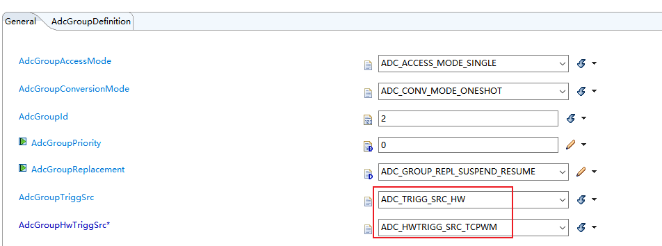
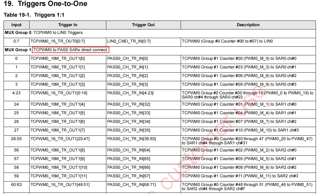
根据手册 35.6.2 Triggers,tcpwm触发adc是一对一的专用触发:
A trigger for a group will cause the acquisitions, as defined by the configurations of the channels in the group, to be executed. There is one dedicated (one-to-one) trigger input for each channel of each of the ADCs connected to the trigger outputs from corresponding TCPWM.
通过组中的通道的配置,待执行。对于每个adc连接到来自相应TCPWM的触发器输出的每个通道,都有一个专用的(一对一的)触发器输入。
gpt配置对应通道的tcpwm。
评论区